1: EBL (tier 3)
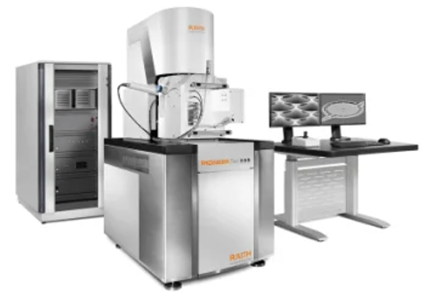
E-Beam Lithography (EBL)
-RAITH / Pioneer 2
PIONEER Two complements thermal field emission (TFE) technology-based Electron Beam Lithography (EBL) tools featuring the smallest beam size in the world within a professional EBL system (< 1.6 nm), sub-8 nm nanolithography performance, optimum mark recognition capabilities and SEM imaging (ET-SE & inlens SE detectors) with crisp contrast and ultimate surface sensitivity. Highest-precision Laser Interferometer Controlled Stage with integrated rotation and tilt functionality is for samples up to 2 inches and fully compatible with all available sample holders.
2: DWL (tier 1)
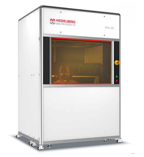
Direct Write Laser Lithography (DWL 66+)
-Heidelberg / DWL 66+
The DWL 66+ laser lithography system is a high-resolution pattern generator for direct writing. This system features powerful options such as front- and backside alignment and 375 nm laser wavelength. The DWL 66+ includes the pneumatic autofocus system as a standard feature and the optical autofocus system additionally for the High-Resolution Mode with a resolution of 300 nm. The optical autofocus will provide superior focus stability and enables the system to expose on surfaces as small as 5x5 mm2. Maximum substrate size and write area are 9”x9” and 200x200 mm2, respectively.
3: Mask Aligner (tier 1)
Contact Mask Aligner
-Karl SUSS / MA6
Mask Aligner is Karl SUSS Model MA-6. This Aligner is a contact printer capable of 1 micron resolution or better, using standard lithographic techniques. Substrates up to 6" in diameter can be used with tooling available for small sample pieces. The mask aligner places an image onto the substrate with precision alignment capability and then exposes the photosensitive resist through a mask with ultra-violet light. The substrate is subsequently developed, exposing the specific pattern for further etching or plating processes. Alignment is achieved manually to an accuracy of <0.25 microns. Alignment modes include vacuum contact for highest resolution and soft contact for minimum substrate damage.
4: ADCS (tier 2)
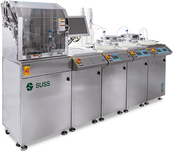
Automatic Dispense Coating System (ADCS)
-SUSS / MCS 8
SUSS’s Manual Coating System (MCS 8) offers the latest generation of coating and aqueous developing techniques in a unique cluster configuration. It is designed and assembled to provide the greatest variety of functionalities on the smallest cleanroom footprint. Our MCS8 consists of two RCD8 modules (Gyrset coater and Developer), hot plate and vapor primer. All modules are equipped with automatic dispensing systems for e-beam and photo resists and developers on wafers up to 4” and substrates up to 6”x6”.
5: EBE 1 (tier 2)
E-Beam Evaporator 1
-FerroTec Temescal / BJD-FC 2000
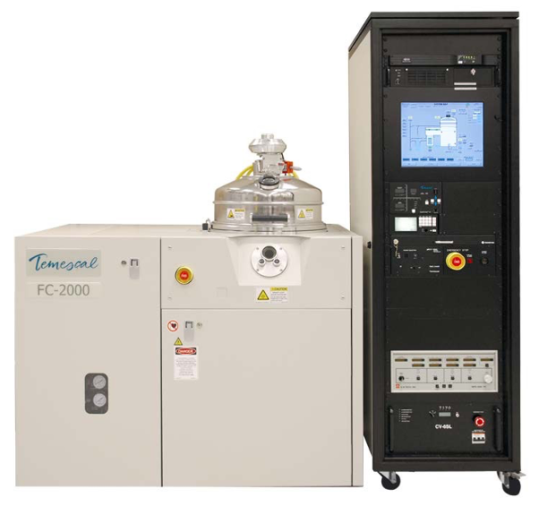
Temescal’s BJD-FC-2000 is a fast-cycle, load- locked evaporation system that allows the source to remain under vacuum during substrate reloading. An 18-inch diameter source isolation valve placed between the source and substrate areas allows not only faster mechanical pump down and production cycle exchanges of wafers, but also minimizing the exposure of hot sources to room humidity and atmospheric contamination. 10 kW e-beam gun is available with 8 pockets of 15 cc configuration. 4” wafers can be loaded up to 13.
6: EBE 2 (tier 1)
E-Beam Evaporator 2
-Temescal / BJD 1800
E-Beam Evaporator 2 is designed for Universities and Research and Development operations. The systems focus a beam of electrons onto a metal target in a crucible to apply a thin metal film onto substrates by evaporation in a high vacuum. The thickness is controlled by electronic feedback systems, and specific tooling geometries allow excellent coverage to be achieved on a variety of substrate sizes up to a diameter of 4''. A total of 7 four-inch wafers can be processed per run. EBE 2 must be operated in auto deposition mode only with gold, chrome, titanium, palladium, aluminum or nickel. The user just selects the material and final thickness and the tool does the rest.
8: Sputter 1 (tier 1)
Sputter Deposition
-Temescal / BJD 1800
Metal sputtering system 1 is a Temescal BJD 1800 system modified for sputtering. Material is deposited by bombarding a target with energetic ions (typically Ar+). Atoms on the surface of the target are knocked loose and delivered to the substrate, resulting in deposition. Electrically conductive materials can be deposited by a dc power source in which the target acts as a cathode and the substrate(s) are mounted on a system anode. Deposition of dielectric materials requires an RF power source to deliver energy to the argon atoms. The system is equipped with 3 magnetrons each with individual shutters, one DC and one RF power supply. Metals can be co-sputtered to create alloys. Dielectrics are not allowed in this system as configured.
9: Sputter 2 (tier 1)
Sputter Deposition
-AJA / Orion 5
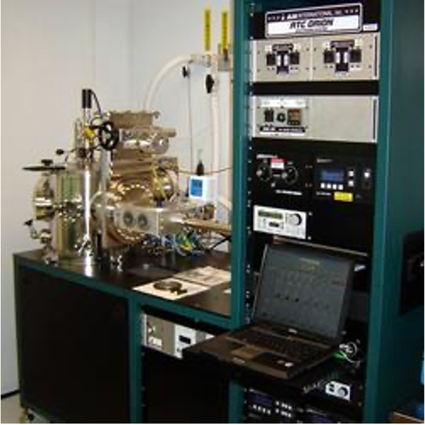
The load-locked AJA ORION 5 Sputtering System currently has five magnetron sputtering sources installed. The system is capable of sputtering individual, sequential or co-sputtering Dielectrics and metals using one RF and one DC power supply. Cycle time exclusive of the deposition period can be as low as 20 minutes due to the load-lock chamber access. Programmable control of deposition parameters and cycling allows automated simultaneous or sequential deposition and repetition of deposition cycles. Substrate rotation up to 20 RPM and heating up to 800 oC is also programmable. The substrate area may also be biased for plasma cleaning prior to deposition. Argon, nitrogen, and oxygen plasmas are possible.
10: ALD (tier 1)
Atomic Layer Deposition (ALD) system
-Cambridge NanoTech / Savaanah 100
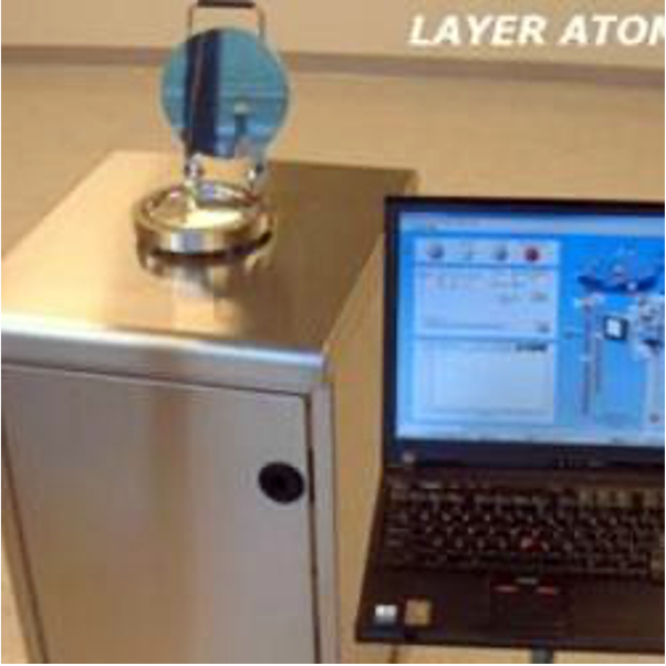
The principle of ALD is based on sequential pulsing of chemical precursor vapors, both of which form about one atomic layer each pulse. This generates pinhole free coatings that are extremely uniform in thickness, even deep inside pores, trenches and cavities. The system accepts a single 4" wafer and the user selects the recipe and the number of cycles to determine the thickness desired. Available precursors include: Aluminum, Zirconium, Hafnium, Gallium and Titanium. Other precursors purchased by the user may be installed by Staff.
11: ALE (tier 1)
Atomic Layer Etching (ALE) system
-Oxford / Plasma Pro 100
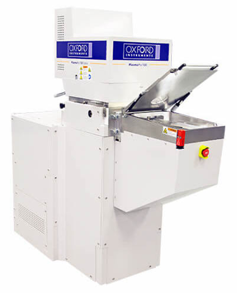
The Plasma Pro 100 ALE delivers precise process control of etching for next-generation semiconductor devices. Specially designed for processes such as recess etching for nanoscale layer etching, the system's digital/cyclical etch process offers low damage, smooth surfaces, and superb etch depth control. Wide temperature range electrode is cooled by a fluid recirculating chiller and resistively heating. RF powered showerhead with optimized gas delivery provides uniform plasma processing. Wafer clamping with He backside cooling allows optimum wafer temperature control. Process gases available are Cl2, SiCl4, BCl3, CH4, H2, HBr, N2, C4F8, SF6, O2, Ar and He.
12: Silicon Etcher
(tier 1)
Silicon Trench Etcher
-Oxford / Plasma Lab 100
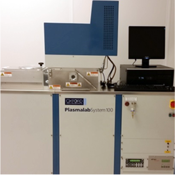
Silicon Trench Etch system accommodates up to 6'' diameter wafers. An inductively coupled plasma (ICP) source produces a high density of reactive species at low pressure. Substrate DC bias is independently controlled by a separate RF generator, allowing control of ion energy according to process requirements. The Cobra module deliver reactive species to the substrate, with a uniform high conductance path through the chamber, allowing a high gas flow to be used while maintaining low pressure. Cryogenic stage cooling is available to deliver extremely smooth sidewall performance and close coupled MFC allow for fast switching of process gasses to achieve very straight high aspect ratio trench etching. Process gases available are N2, C4F8, SF6, O2, Ar and He.
13: Metal Etcher
(tier 1)
Metal Trench Etcher
-Oxford / Plasma Lab 100
Metal Trench Etching System is an ICP plasma etch tool designed for etching trenches in metals, hundreds of microns deep or even completely through a wafer. Although currently optimized for etching titanium this tool is configured with Cl2, BCl3, CHF3, SF6, He, CF4, CHF3 and N2 gases to provide flexibility in etching processes.
14: Ellipsometer
Ellipsometer
-Horiba / UVISEL SPME
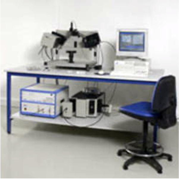
Ellipsometer system is a UVISEL Spectroscopic Phase Modulated Ellipsometer (SPME) that incorporates a photo-elastic device to modulate the polarization without any mechanical movement. The UVISEL FUV extends the range of measurements down to 190 nm. The FUV200 integrates two different detectors (solar blind and UV/Vis PMT detectors) to provide an extremely low level of stray light. Combined with high throughput optics, this ellipsometer provides very high sensitivity and precision without compromise. The FUV range is often required for lithography applications, characterization of metals, high k dielectrics and organic materials as well as increased sensitivity to ultra-thin films.
15: Profilometer
Surface Profilometer
-Veeco / Dektak 8
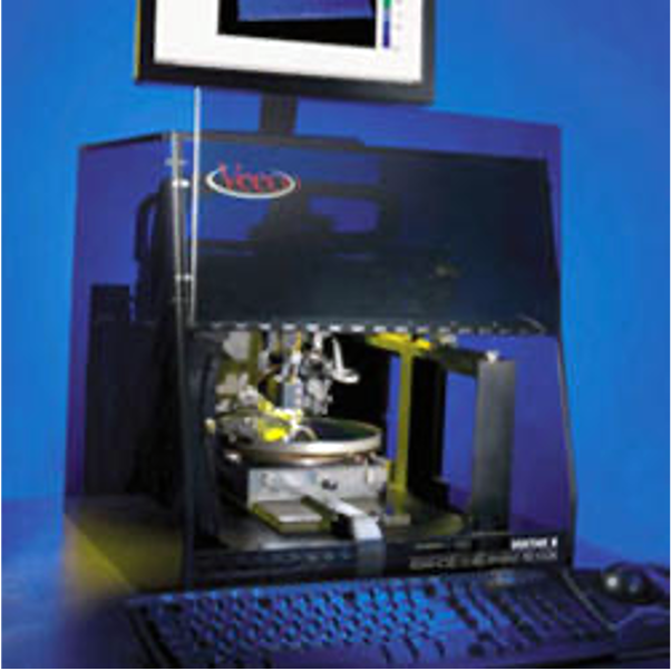
Surface profilometer and thin film stress gauge are combined in one tool - the Veeco system Dektak 8. The system is a bench-top Surface profiler that measures the step heights of any surface, with a programmable stylus, which applies a force down to 1 milligram and a Z-height capability up to 1 millimeter. It has a low- inertia sensor to deliver extremely accurate step heights, surface roughness, and waviness measurements on samples up to 8 inches in diameter. 3D data analysis software for surface characterization of MEMS, semiconductors and other thin/thick films. The system provides 7.5 angstrom, 1 sigma step height repeatability. Stress measurements are achieved by measuring the curvature profile of a substrate before and after a given process step.
16: PPMS (tier 1)
Physical Property Measurement System
-Quantum Design / DynaCool
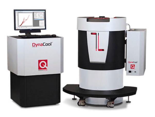
Physical Property Measurement System (PPMS) from Quantum Design is cryogen-free package and uses a single two-stage Pulse Tube cooler to cool both the superconducting magnet and the temperature control system, providing a low vibration environment for sample measurements. It offers continuous low temperature control and precise field and temperature sweep modes. Temperature ranges 1.8 - 400 K. 9, 12, and 14 T magnets are available.
17: STEM (tier 3)
Scanning Transmission Electron Microscope (STEM)
-Thermo Fisher (FEI) / Titan Themis 300
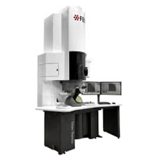
Titan Themis 300 is a state-of-the-art scanning transmission electron microscope. The Titan platform technology, which is unmatched in mechanical, electronic, thermal, and optical stability is designed to deliver ultimate performance in TEM, STEM, diffraction and EDX modes to study nano structures in wide range of materials. The X-FEG electron gun provides high coherence and high brightness combined with stable emission currents for advanced analytical and high resolution applications. The high tension flexibility (60 to 300 kV) allows to optimize the system according to the requirements of the specific experiment and material.
18: TEM (tier 2)
Transmission Electron Microscope (TEM)
-Thermo Fisher (FEI) / Talos L120C
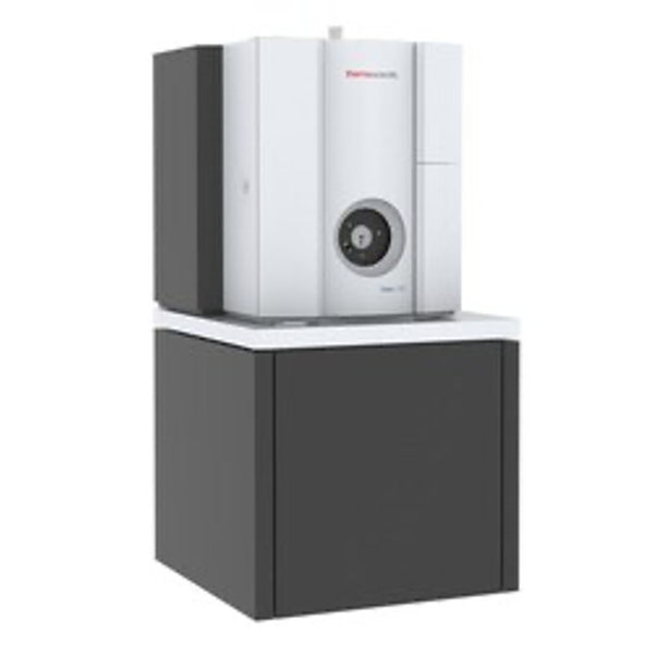
Talos L120CTM TEM is a 20-120 kV transmission electron microscope designed for performance and productivity across a wide range of samples and applications, such as minerals, metals, ceramics, cells, cell organelles, polymers, and any other type of solid materials prepared as thin specimens (<100 nm thickness) or fine nanoparticles both at ambient and cryogenic temperatures. With its motorized, retractable cryo-box and low-dose technique, the imaging quality of beam-sensitive materials is taken to the next level. It is an adequate instrument for a wide range of applications and users, ranging from experienced senior researchers to students just entering the field of TEM.
19: SEM (tier 2)
Scanning Electron Microscope (SEM)
-Thermo Fisher (FEI) / NNS 450
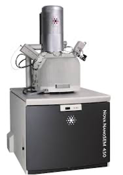
NNS450 combines high- and low-voltage ultra-high resolution capabilities with variable pressure specimen chamber vacuum. Superb contrast and surface sensitivity at low voltages can be achieved using the beam deceleration mode. High-resolution imaging of non-conductive specimens is enabled by utilizing immersion lens mode at low-vacuum. The analytical system allows to perform qualitative and quantitative chemical analysis, image capture, X-ray spectral mapping and line scanning by Energy Dispersive X-ray Spectroscopy (EDX) complemented by structural and crystallographic information including crystal orientation and mis-orientation, accurate phase identification, and phase mapping by Electron Backscattered Diffraction (EBSD).
20: SEM-FIB (tier 2)
Focused Ion Beam (FIB)
-Thermo Fisher (FEI) / Quanta 3D 200i
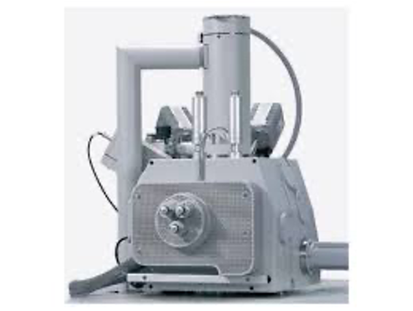
QuantaTM 3D 200i combines a scanning electron microscope (SEM) with a high current focused ion beam (FIB) to to precisely prepare samples for 3D nanoanalysis, TEM, EBSD & atom probe imaging or structural modification of sample surfaces at nanometer scale by removing or depositing material at a rapid rate in small defined areas. Quanta 3D features three imaging modes – high vacuum, low vacuum and ESEMTM it can accommodate the widest range of samples of any SEM system. Charge neutralization mode is integrated for working with FIB on insulating samples.
21: SEM-RISE (tier 2)
Raman Imaging and Scanning Electron Microscope (RISE)
-TESCAN / Mira 3
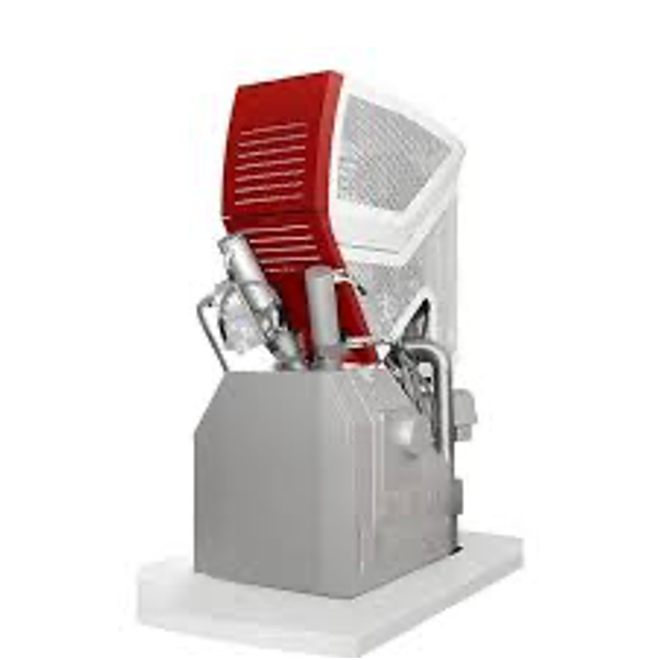
The MIRA3 utilizes unique 4-lens electron optical design that provides a wide range of imaging and scanning modes, including: high resolution imaging (Resolution mode), ultra-low magnification imaging (Wide Field mode), high depth of field imaging (Depth mode), Live 3D Stereoscopic imaging, and Selected Area Electron Channeling (beam rocking for acquisition of electron diffraction images). Mira3 SEM is fitted with dual Energy Dispersive Spectrometer (EDS) system with large area elemental mapping capabilities and 3D surface rendering system as well as with a confocal Raman microscope for comprehensive correlative sample analysis.
22: Vitrobot (tier 1)
Cryo-TEM Sample Preparation
-Thermo Fisher / Mark iV
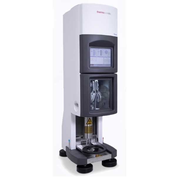
Vitrobot Mark IV System offers semi-automated vitrification to provide fast, easy, and reproducible sample preparation for cryo-TEM. It performs the cryo-fixation process at constant physical and mechanical conditions like temperature, relative humidity, blotting conditions, and freezing velocity. This ensures high-quality cryo-fixation results and a high sample preparation throughput prior to cryo-TEM observation.
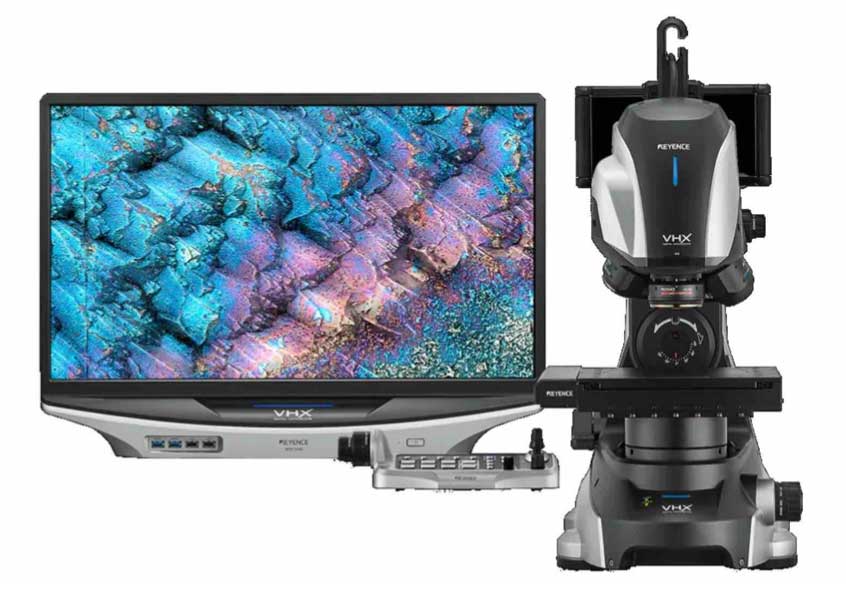
23: DLM (tier 1)
Digital Light Microscope
-Keyence / VHX-7000
The VHX-7000 Series is a fully-automated digital light microscope system that enables even novice users to capture high-resolution images. It can operate as a light microscope to image transparent samples on a microscope slide, or render 3D mapping surface topography of nontransparent samples like a simplified scanning electron microscope. It uses a 4K CMOS sensor.
